物料型号包括:IPD04N03LA、IPF04N03LA、IPS04N03LA、IPU04N03LA。
这些是OptiMOS®2系列的功率晶体管。
器件简介:OptiMOS®2系列的N沟道逻辑电平功率晶体管,具有优秀的门电荷x R_DS(on)产品(FOM),卓越的热阻,175°C工作温度,无铅引脚镀层,符合RoHS标准。
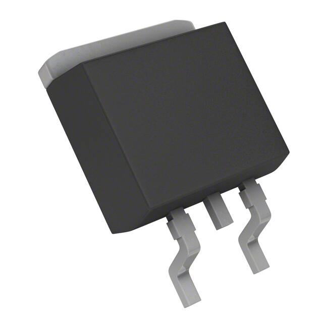
引脚分配:这些器件是3引脚的P-TO252-3-11、P-TO252-3-23、P-TO251-3-11、P-TO251-3-1封装,排列为漏极引脚2、栅极引脚1、源极引脚3。
参数特性包括:连续漏极电流、脉冲漏极电流、雪崩能量、反向二极管dv/dt、栅源电压、总功耗、工作和存储温度范围等。
功能详解:包括热特性、电气特性(静态特性、动态特性)、反向二极管特性、雪崩特性等。
应用信息:适用于需要高功率、高效率和高温操作的场合。
封装信息:提供了不同封装类型的详细尺寸和公差,例如PG-TO252-3-11、PG-TO252-3-23、PG-TO251-3-11、PG-TO251-3-21。
以上信息摘自英飞凌技术的数据手册。